Built in potential in pn junction diode Diode avalanche zener breakdown junction biased semiconductor unbiased explained phenomenon studiousguy diodes Schematic diagram of forward biased diode
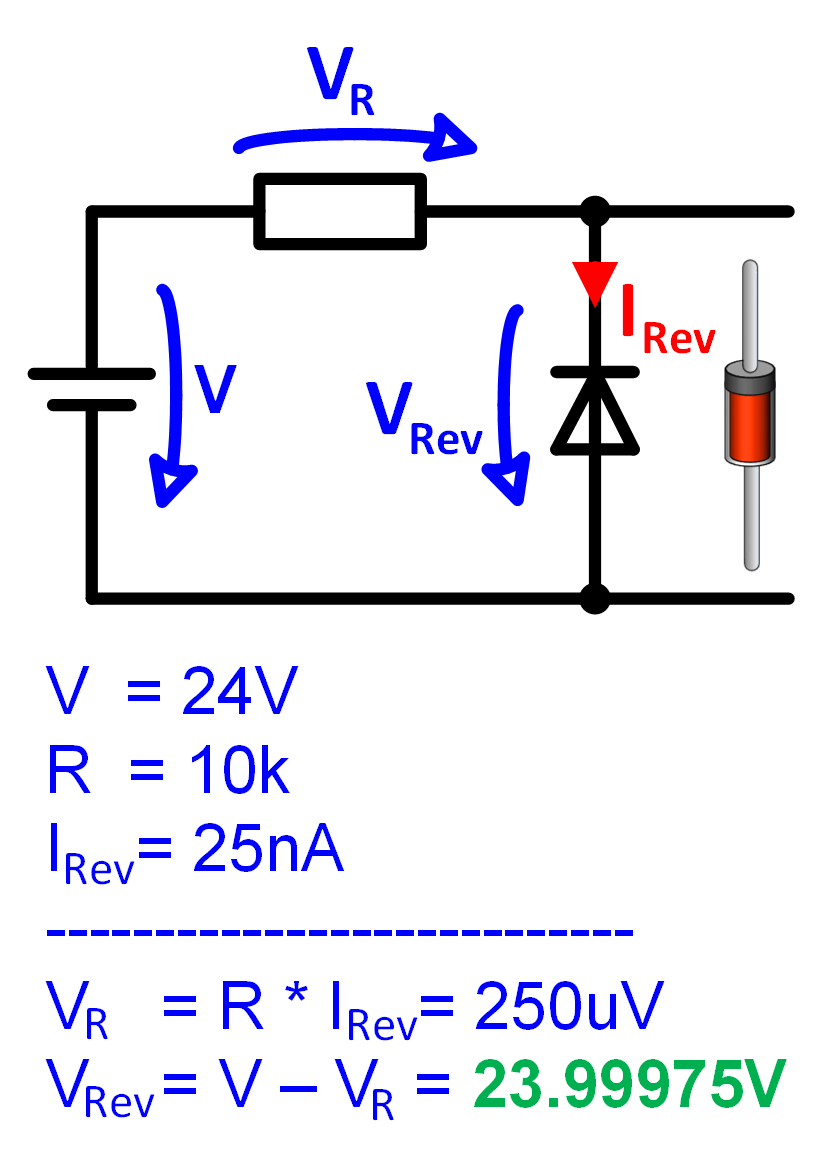
Electronic – Voltage drop – Diode reverse biased – Valuable Tech Notes
Schematic diagram of forward biased diode Pn junction diode and vi characteristics » pija education Schematic diagram of forward biased diode
Diode forward bias circuit diagram » circuit diagram
Index [merberich.github.io]Forward bias, reverse bias and their effects on diodes Cbse class 12 physics chapter 14 revision notesForward bias circuit diagram.
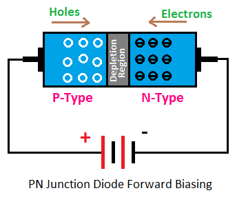
Forward and reverse bias of a pn junction explained electrical4uDiode in forward and reverse bias Electronic – voltage drop – diode reverse biased – valuable tech notesForward biasing of pn junction diode.
Fogebrity mastermind
Forward and reverse bias circuit diagramDiode reverse junction bias pn biased under forward depletion layer condition due biasing characteristics semiconductor increase region showing gif when Zener diode forward bias circuitDiode circuits bias diodes voltage divider.
Multisim bias diode zenerDiodes and diode circuits Schematic diagram of forward biased diodePn junction diodes (l-iv) – m dash foundation: c cube learning.
Forward biased circuit diagram
☑ define unbiased diodeWhat is zener diode? its principle working and example usage Diode replacement chartZener diode forward and reverse bias simulation.
Diode pn junction zener forward bias difference between circuit chart depletion notForward biasing of pn junction diode Diode diodes voltage current real relationship sparkfun curve characteristics non plot linear negative learn equal positive looks bothPn junction bias diode diodes.

Circuit diagram of zener diode in forward bias
Difference between pn junction & zener diode (with comparison chartSchematic diagram of forward biased diode Diode forward bias circuit pn junction characteristics battery circuitsPn junction diode and diode characteristics.
Diode bias calculation figureSemiconductor diode forward bias Difference between forward reverse biasing with comparison chart imagesIn a p.

Forward and reverse bias of a pn junction explained electrical4u images
.
.


Forward Biased Circuit Diagram

Forward Biasing of PN Junction Diode - Definition, Theory & Diagram

PN JUNCTION DIODE AND VI CHARACTERISTICS » PIJA Education

Zener Diode Forward and Reverse Bias Simulation

☑ Define Unbiased Diode

Zener diode forward bias circuit - Multisim Live

Electronic – Voltage drop – Diode reverse biased – Valuable Tech Notes
